News
2024/12/16
DNP Achieves Fine Pattern Resolution on EUV Lithography Photomasks for Beyond 2nm Generation
Commences sample supply of high-NA EUV photomasks for next-generation semiconductors

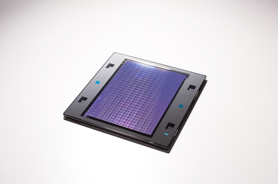
Tokyo, December 12, Dai Nippon Printing Co., Ltd. (DNP) has successfully achieved the fine pattern resolution required for photomasks for logic semiconductors of the beyond 2nm (nm: 10-9 meter) generation1 that support Extreme Ultra-Violet (EUV) lithography, a cutting-edge process in semiconductor manufacturing.
DNP has also completed the criteria evaluation for photomasks compatible with High-Numerical Aperture2, the application being considered for next-generation semiconductors beyond the 2nm generation, and has commenced the supply of evaluation photomasks to semiconductor development consortia, manufacturing equipment manufacturers, and material manufacturers. High-NA EUV lithography makes it possible to form fine patterns on silicon wafers with a higher resolution than previously possible, and is expected to lead to the realization of high-performance, low-power semiconductors.
In recent years, advances have been made in the mass production of cutting-edge logic semiconductors using EUV lithography with an EUV light source. Expanded adoption has also been seen in memory semiconductors, making EUV lithography essential in the supply of cutting-edge semiconductors.
DNP completed the development of a photomask manufacturing process for 3nm generation EUV lithography in 20233, and followed this up in 2024 by participating as a subcontractor in the Post-5G Information and Communications System Infrastructure Strengthening Research and Development Project of the New Energy and Industrial Technology Development Organization (NEDO), a national research and development agency. Tokyo-based Rapidus Corporation (Rapidus) is also a participating member of this project, and we have been developing technologies related to the photomask manufacturing process and guarantees for cutting-edge logic semiconductors to Rapidus4.
Development
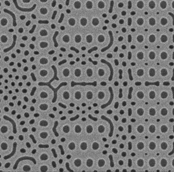
DNP has now achieved the fine pattern resolution required for EUV lithography photomasks for logic semiconductors of the beyond 2nm generation. DNP has also completed the development of EUV photomasks compatible with High-NA, being considered for next-generation semiconductors beyond the 2nm generation, has completed the criteria evaluation for EUV photomasks, and commenced supply of sample masks.
・To realize photomasks for beyond 2nm generation EUV lithography, requires patterns 20% smaller than those for the 3nm generation. This refers not only to the size and shape of the patterns, and technology required to resolve fine patterns of all types on the face of the same mask. This includes not only standard straight and rectangular patterns but also increasingly complex curved patterns. DNP has achieved the pattern resolution required for the beyond 2nm generation by making repeated improvements based on the established 3nm generation manufacturing process.


・Photomasks for high NA-EUV lithography require higher precision and finer processing than those for standard EUV lithography. DNP established and optimized a manufacturing process flow that differs from that for conventional EUV lithography photomasks.
Going Forward
DNP will continue to establish production technologies, such as for improving manufacturing yields, with the goal of commencing mass production of photomasks for 2nm generation logic semiconductors in FY 2027.
We will also continue to cooperate with imec, a cutting-edge international research organization headquartered in Leuven, Belgium to promote the development of photomask manufacturing technologies with an eye toward the 1nm generation.
DNP will continue to contribute to the growth of Japan's semiconductor industry by promoting development in collaboration with various partners within the framework of the international semiconductor industry.
1: Compliant with International Roadmap for Devices and Systems (IRDS) standards
2: Numerical Aperture (NA) is a number that indicates the brightness and resolution of an optical system. High-NA refers to the expansion of the lens NA of EUV exposure equipment from the conventional 0.33 to 0.55.
3: https://www.global.dnp/news/detail/20170124_4126.html
4: https://www.global.dnp/news/detail/20173706_4126.html
*Company and product names listed in this release are the trademarks or registered trademarks of those companies.
*Product specifications and service details referred to in this news release are current as of the date of the announcement. They may be changed without notice.
- Category
- Headline News

